

Under normal circumstances, all components should be arranged on the same side of the circuit board. Only top-mounted components that are too dense, such as surface-mount resistors, surface-mount capacitors, and surface-mount ICs with limited height and low heat generation can be placed on the bottom.
Components should be placed on the grid and arranged in parallel or perpendicular to each other to achieve a neat and beautiful appearance, while still ensuring their electrical performance. In general, components should not overlap. The arrangement of components should be compact, and their distribution throughout the entire board should be uniform and balanced.
The minimum distance between adjacent pad shapes of different components on the circuit board should be greater than 1 millimeter.
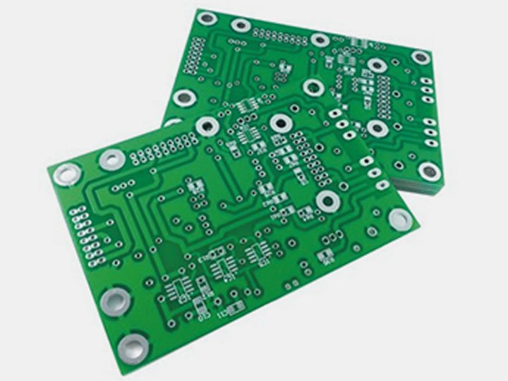
The distance from the edge of the circuit board should generally not be less than 2mm. The optimal shape of the circuit board is rectangular, with a length-to-width ratio of 3:2 or 4:3. When the size of the circuit board is greater than 200mm*150mm, its mechanical strength should also be considered.
In the PCB fabrication layout design process, each functional unit of the circuit board should be analyzed and the layout design should be based on its function. When designing the layout of all circuit components, the following principles should be followed:
Arrange each functional unit's respective circuit elements according to the flow of the circuit, making the layout conducive to signal flow and as consistent as possible in direction.
Layout around the core components of each functional unit. Components should be arranged uniformly, compactly, and collectively on the printed circuit board, with their leads and connections minimized and shortened as much as possible.
For circuits operating under high-frequency conditions, the distribution parameters between components must be considered. General circuits should try to arrange the components in parallel, not only beautiful but also easy to assemble and mass-produce.
Special components in PCB design refer to key components in high frequency modules, core components in circuits, sensitive components, high voltage components, high heating components, and some special-shaped components. The layout of these special components must comply with the requirements of circuit functions and production needs. Poor placement may cause compatibility and signal integrity issues, leading to PCB design failure.
When placing special components in the design, the size of the PCB should be considered first. If the PCB size is too large, the printed circuit line will be longer, the impedance will increase, the anti-interference ability will decrease, and the cost will increase. If it is too small, heat dissipation will be poor and adjacent circuits may be easily affected by interference. After determining the size of the PCB, the placement positions for special parts should be determined. Finally, layout all components according to the functional unit.
Place components that fit closely with the structure, such as power sockets, indicator lights, switches, and connectors.
Place special components such as large components, heavy components, heating components, transformers, integrated circuits and so on.
Place small components.
Check whether the PCB size matches the processing dimensions required by the drawing.
Check whether the component layout is balanced, arranged neatly and whether all components have been arranged.
Check for conflicts at all levels. For example, whether the components, frames, and layers that need to be privately printed are reasonable.
Check whether commonly used components are easy to use, such as switches, plug-in boards, and components that need to be replaced frequently.
Check whether the distance between thermosensitive components and heating components is reasonable.
Check whether the heat dissipation is good.
Check whether the circuit's interference problem needs to be considered.