The PCB design is the process to convert a circuit schematic into a diagram of bms PCB and determine processing technical requirements according to the intent of designers, which is generally divided into two ways of manual design and computer-aided design. The current PCB design basically uses computer-aided design because the structure of modern electronic products is more and more complex. Its process includes:
(1) Select the material of bms PCB and determine the whole machine structure.
(2) Consider the installation, location and size of electric, machinery and components.
(3) Determine the width and spacing of wires, the diameter and aperture of pads.
(4) The structure of design custom PCB is printed plug or connector.
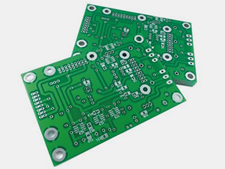
Start from determining the size of bms PCB. The size which is limited by a case should be appropriate to fix bms PCB into case. In addition, the connection method of bms PCB and external components( mainly potentiometers, sockets or external bms PCBs) should be considered.
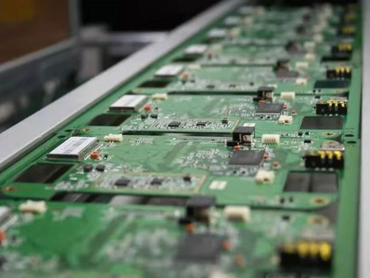
The bms PCB and external components are generally connected by plastic wires or metal shielding wires, but sometimes they are also designed in the form of sockets, i.e., installing a plug-in bms PCB in a device and leaving a contact position acting as a socket. For larger components fixed on bms PCB board, it is necessary to add metal components to improve vibration resistance and impact resistance.
Firstly, we need to have a complete understanding of the specification, size, area of various sockets. It is also necessary to reasonably and carefully consider the location of each component, mainly from the compatibility and anti-interference of electromagnetic field, short track, less crossing, path and destination of power supply and ground, etc. : After fixing the position of each component, we should consider the connection of components. According to the relevant pins of circuit diagram connection, there are two types of computer-aided mapping and hand-aligned layout, of which the most original is hand-aligned layout.
This method is more troublesome because it often needs to repeat several times to finalize. It is usually for those without other drawing equipments. Hand-aligned layout is also very helpful for designers just learning printed layouts. For computer-aided mapping, there are many drawing softwares with various functions now, but in general, computer-aided mapping is more convenient to draw and modify and can be saved and printed.
Secondly, we need to determine the size required for bms PCB and according to the schematic, initially determine the position of each component, and then the layout will be more reasonable through constant adjustment.
HX Electronic Technology PCB assembly suppliers provide fast, professional and high-quality service, including at least 6-hour quotation release, at least 2-hour engineer query release, at least 72-hour and at least 48-hour global express, 2 hours to solve after-sales problems, professional DFM report and 24-hour online customer service. Please feel free to contact us.