
1. The edges of the input end and output end of the theremin PCB should be perpendicular to each other
The edges of the input end and the output end should be avoided adjacent and parallel to avoid reflection interference. If necessary, ground wire should be added for isolation, and the wiring of two adjacent layers should be perpendicular to each other. Parasitic coupling is easy to occur in parallel.
2. Add decoupling capacitors between the power and ground wires of the theremin PCB
Widen the width of the power and ground wires as much as possible, preferably the ground wire is wider than the power wire, their relationship is: ground wire>power wire>signal wire, usually the signal wire width is: 0.2~0.3mm, the finest width can reach 0.05 ~0.07mm, the power cord is 1.2~2.5mm.
3. Common ground processing of the digital circuit and the analog circuit of the theremin PCB
The frequency of the digital circuit is high, and the sensitivity of the analog circuit is strong. For the signal line, the high-frequency signal line should be as far away as possible from the sensitive analog circuit device. For the ground line, the entire PCB has only one node to the outside world, so it must deal with the problems of digital, analog, and common ground inside the PCB.
Inside the board, the digital ground and the analog ground are actually separated, and they are not connected to each other, but at the interface (such as a plug, etc.) connecting the PCB theremin circuit board to the outside world.
There is a short connection between digital and analog. Please note that there is only one connection point, and there are some that do not share the ground on the PCB. This is determined by the system design.
4. Shorten the wiring between theremin PCB and high-frequency components, reduce distribution parameters and mutual electromagnetic interference.
Components that are susceptible to interference should not be too close to each other, and input and output components should be kept as far away as possible. There may be a high potential difference between some components or wires, and the distance between them should be increased to avoid accidental short circuits caused by discharge.
Components with high voltage should be placed as far as possible in places that are not easy to reach during debugging. For circuits that work at high frequencies, the distribution parameters between circuit board components should be considered.
Generally, the circuit should be arranged in parallel as much as possible. In this way, it is not only beautiful, but also easy to install and weld, and easy to mass production.
1. According to the current of the printed circuit board, try to increase the width of the power line and reduce the loop resistance. At the same time, make the direction of the power line and the ground line consistent with the direction of data transmission, which helps to enhance the anti-noise ability.
2. The principles of ground wire design are:
(1) The digital ground is separated from the analog ground. If there are both logic circuits and linear circuits on the circuit board, they should be separated as much as possible.
The ground of the low-frequency circuit should be single-pointed and connected to the ground as much as possible. When the actual wiring is difficult, the circuit board can be partially connected in series and then connected to the ground. The high-frequency circuit should be grounded at multiple points in series, the ground wire should be short and leased, and the grid-like large-area ground foil should be used around the high-frequency component as much as possible.
(2) The grounding wire should be as thick as possible. If a long line is used for the ground wire, the ground potential changes with the current, which reduces the noise resistance. Therefore, the circuit board ground wire should be thickened so that it can pass three times the allowable current on the printed board. If possible, the grounding wire should be 2~3mm or more.
(3) The grounding wire forms a closed loop. For printed boards composed of only digital circuits, the grounding circuits are mostly arranged in closed loops to improve noise immunity.
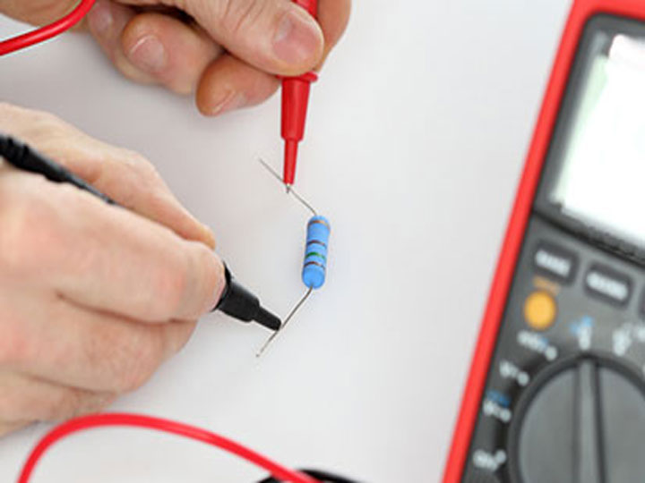
3. Theremin PCB decoupling capacitor configuration: One of the conventional methods of design custom PCB is to configure appropriate decoupling capacitors on each key part of the printed board.
The general configuration principles of decoupling capacitors are:
(1) Connect a 10~100uf electrolytic capacitor across the power input. If possible, it is better to connect to 100uF or more.
(2) In principle, each integrated circuit chip should be equipped with a 0.01pF ceramic capacitor. If the gap of the circuit board is not enough, a 1-10pF capacitor can be arranged for every 4~8 chips.
(3) For devices with weak anti-noise ability and large power changes when shutting down, such as RAM and ROM storage devices, a decoupling capacitor should be directly connected between the power line and the ground line of the chip.
(4) Capacitor leads should not be too long, especially for high-frequency bypass capacitors.