When creating the best circuit board design, one of the factors that must be considered is the solder resist layer and whether to use a matte finish or bright finish. Most manufacturers will default to the illuminated surface, which is the most popular choice of the two.
The main difference between the two types is aesthetics. Glossy solder will have light reflection and lighter color, while matte is dull and dark. The matt solder resists being softer, while the bright light has a strong shell finish. In PCBA(printed circuit board assembly) manufacturing, there is no difference in the process. If any, the cost of design custom PCBdifference is tiny.
Matte finishes may be more easily scratched due to soft finishes, but scratches are more evident on bright finishes. However, due to the high reflectivity, there may be problems in the visual system during the assembly of the glossy solder mask by PCB assembly suppliers. When using glossy film, the film removal around the reference point plays an essential role in the optical system.
1. Glass transition temperature.
2. Surface energy.
3. Hardness.
4. Flux type.
5. There is moisture.
6. Surface roughness.
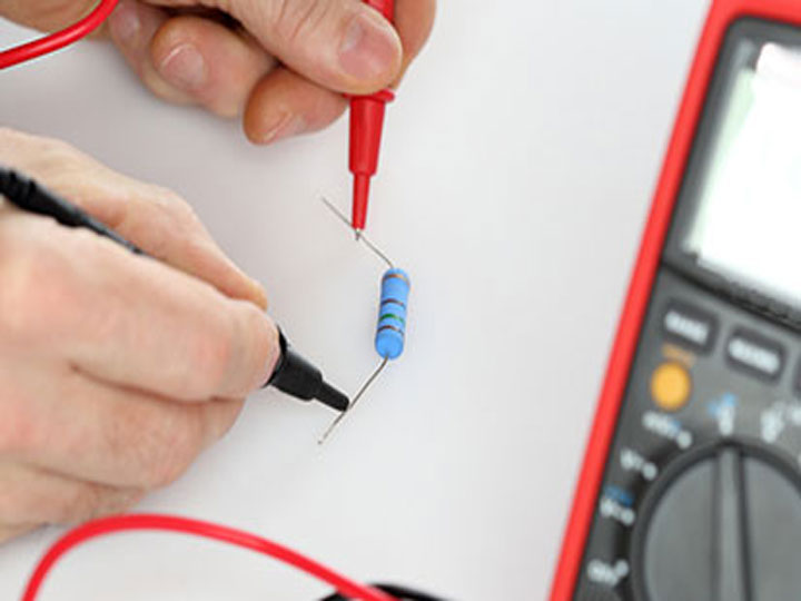
Although surface roughness has always been a specific factor in the production of solder balls, its exact mechanism has not been fully understood. Molten solder with a rough (matte) surface is different from molten solder with a smooth surface - used for masks and laminates of various PCB solders. The molten solder forms a convex meniscus on the rough surface, and on the smooth surface, the molten solder forms a concave meniscus. Convex and concave surfaces reduce the attachment area of the solder ball, so the solder ball will not adhere to the matte surface like a smooth surface.
Many studies on gloss level and its correlation with welding defects show that the gloss of photo imaging will affect the number of welding defects in the wave soldering process of PCBA. These welding defects are directly proportional to the glow. With the decrease of gloss, the reduction of solder ball level is faster than the number of welding short circuits and bridges. In other words, to reduce or eliminate solder short circuit, the required gloss is lower than that needed to reduce solder ball.